
Flex PCBs Handle Vibrations and Shocks
Flex circuits are used in a wide variety of applications to provide electrical connections between flexible components and rigid components. They are also used to replace wire harnesses, which are heavier and bulkier and difficult to manufacture, and are often used in applications with dynamic bending such as folding cell phones (dynamic application).
The use of flex PCBs can provide substantial weight reduction for the final product, while increasing durability and allowing for more efficient routing. The key to achieving this is to consider all the requirements for the circuit board’s operating environment during design and prototyping, including vibrations and shocks. The following tips can help ensure that your flex circuits will be able to handle these environmental conditions.
During the prototyping stage, it is important to use simulation software to determine the maximum amount of flexing that will be possible. In addition to this, a physical prototype can be built and used to test the functionality of the flex circuit boards. This will allow for any potential issues to be identified and corrected before production begins, saving both time and money.
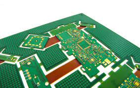
How Do Flex PCBs Handle Vibrations and Shocks?
When designing a flex circuit, it is important to pay attention to the material selection process. The choice of the material will have a direct impact on how much your circuits can flex. A high-quality flex circuit should be made from roll annealed copper, which is less brittle than ED (deposited) copper. It is also important to call out the copper grain direction on your fabrication drawing, which will help to minimize damage during forming.
Another important consideration for flex circuits is the bend radius. The minimum angle at which the flex area can be bent should be determined early in the design phase to prevent damage to the copper. Avoiding tight bends is key, as they can cause stress points that will eventually lead to failure in the circuit. Instead, you should aim to achieve gradual and large curved angles when determining the flex radius. It is also important to stagger the conductors in multi-layered flex circuits and to route them perpendicular to the bend axis. This will eliminate the stress points that are created by stacked copper and will help to minimize breakage of the copper.
Rigid-flex circuits can require a more complex layer stack than traditional rigid boards due to the addition of the flex section. It is important to plan the layer stack for both rigid and flex sections carefully using your PCB layout software. This will help to reduce the number of stiffeners needed in areas that are likely to experience a lot of bending, as well as ensuring that the proper impedance is maintained through transitions in trace width. It is also a good idea to include stiffener locations on your fabrication drawings for easy identification.